Quantum Tech: The Next Frontier in Lithography?
The semiconductor industry is entering a period of radical convergence, where physics, chemistry, and computation are being reimagined at the smallest imaginable scales. With conventional lithography techniques nearing physical and economic boundaries, researchers are beginning to explore how quantum technologies could redefine not only computation but also the processes that create the chips themselves. During the SPIE lithography conference, Erik Hosler, a seasoned consultant and former EUV lithography expert, captured this paradigm shift, framing it as part of a broader, industry-wide awakening to the future of fabrication.
While Moore’s Law may no longer dictate the pace of progress, the quest for performance, precision, and efficiency continues. Quantum science is emerging as a potential enabler, not only as an eventual replacement for classical logic but also as a tool for improving the methods used in nanoscale manufacturing. The question now facing the semiconductor world is no longer whether quantum technologies will be relevant but how soon and in what form they will begin to influence the lithography roadmap.
A Convergence of Disciplines
For much of its history, semiconductor lithography has relied on precise but classical principles involving light, optics, and chemistry to define transistor features. But as critical dimensions shrink and pattern fidelity becomes more difficult to control, quantum phenomena such as tunneling, entanglement, and energy quantization are no longer merely side effects. They are active constraints and potential future assets.
Today’s most advanced lithography tools, such as Extreme Ultraviolet (EUV) systems, already contend with quantum scale effects. Photon shot noise and stochastic resist interactions are driven by quantum-level events that limit reliability and yield. The deeper researchers investigate these effects, the more apparent it becomes that quantum behavior is not just a challenge but a potential guide to the next generation of lithography solutions.
Quantum Aware Resist Development
One of the most promising intersections between quantum physics and lithography lies in materials science. At the forefront are photoresists, the light-sensitive materials used to transfer patterns onto wafers. These resists are now being engineered with quantum interactions in mind, especially for next-generation EUV and high Numerical Aperture (high NA) systems.
Traditional Chemically Amplified Resists (CARs) are reaching performance limits under EUV exposure. The photon energy involved is so high that it triggers complex, probabilistic events in the resist layer, leading to unpredictable outcomes. To address this, researchers are exploring new molecular resists and metal oxide materials that react more predictably and may leverage quantum behavior such as discrete energy level absorption.
Some of these materials are being evaluated in specialized research labs using ultrafast laser pulses to observe electron dynamics during exposure. This field, known as ultrafast spectroscopy, is helping researchers better understand the resist response to EUV photons on attosecond and femtosecond timescales. The goal is to design resist chemistries that not only deliver higher resolution and sensitivity but also behave consistently under the influence of high-energy quantum events.
Precision Measurement in a Quantum World
As feature sizes approach the atomic scale, metrology and inspection face new obstacles. Traditional optical microscopes and scanning electron microscopes with the resolution and accuracy required for next-generation chips prompted the exploration of quantum-based measurement technologies.
Quantum sensors that exploit phenomena like coherence and superposition are being investigated for use in materials characterization and nanoscale inspection. These sensors could detect incredibly slight changes in electric or magnetic fields, enabling precise defect identification and process monitoring.
In parallel, techniques such as quantum interferometry are being explored to enhance surface profiling and structural analysis. Though not yet widely adopted in semiconductor fabrication, these quantum-enhanced metrology approaches could one day supplement or even surpass current tools in both sensitivity and resolution.
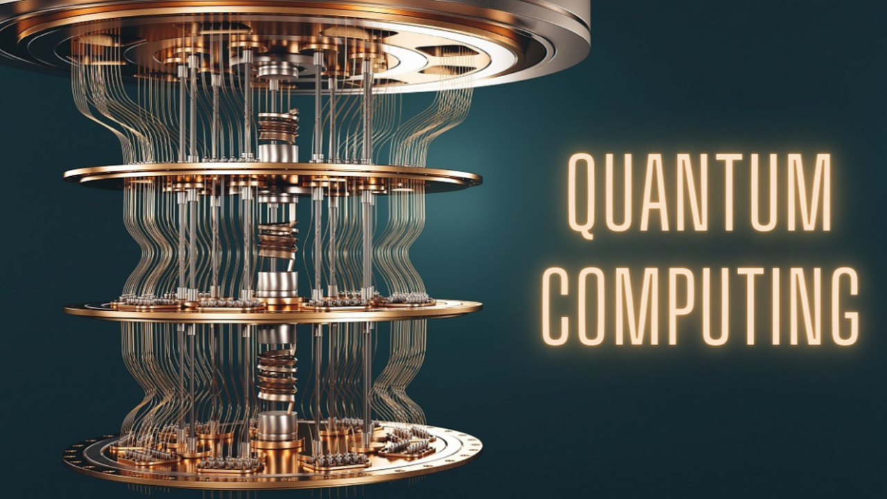
The Fabrication Path to Quantum Chips
There is also a direct connection between lithography and the fabrication of quantum computing devices. As companies race to build scalable quantum processors, they require extreme precision in materials, patterning, and environmental control. Whether working with superconducting qubits, photonic circuits, or spin-based systems, the fabrication challenges are immense.
Quantum hardware demands lithographic precision at the nanometer level, with ultra-low defect densities and highly uniform material properties. Even minute contamination can cause decoherence or gate errors. As a result, fabs developing quantum chips incorporate techniques such as atomic layer deposition, cryogenic processing, and ultra-cleaning etch environments.
These advanced capabilities, developed initially to support quantum technologies, could eventually feed back into classical semiconductor production. Lessons learned from building quantum devices may improve control and yield in processes that also benefit conventional chipmaking.
A Broader Agenda for Exploration
At the SPIE conference, the widening scope of topics reflects the growing complexity of semiconductor advancement. Where lithography discussions once centered around optics and exposure systems, they now include quantum sensing, advanced materials, and even quantum computing itself.
Erik Hosler notes, “Last year, we included MEMS and MOEMS, and we will keep expanding to quantum to make this a place to ask questions … Lots of great things are going on, and something will emerge.”
The inclusion of quantum topics at SPIE reflects a shift in mindset in how the semiconductor community approaches innovation. Instead of seeing quantum science as a separate domain, industry leaders are beginning to view it as part of the broader roadmap. Whether used to fabricate quantum chips or improve existing processes, quantum technologies are becoming tools in the lithographer’s kit.
Outlook: From Possibility to Practice
Quantum technologies are not ready to replace conventional lithography systems, but they are beginning to inform how the next generation of tools and materials will change. As researchers and engineers better understand quantum interactions in resists, metrology, and device design, they are laying the groundwork for a future where quantum and classical approaches coexist.
That is not a departure from proven methods but an expansion. By bringing quantum perspectives into lithography, the industry opens new pathways to overcome challenges that classical physics alone can no longer fully address. The next leap in patterning may not be about shrinking wavelengths or increasing doses but about learning how to work with matter at its most fundamental level.